Preface#
This article is a build log of my first bare-metal experiments on the nRF52840. If you are new to embedded systems,
it may help you understand what happens before main() and how simple peripherals are controlled through registers. Dig
in!
Why I Started with Bare-Metal#
I am a beginner in embedded systems programming, and I wanted to better understand the nRF52840 MCU. And what better way to do that than by writing a few bare-metal programs for it? So, before starting the nRF52840 web server, I wrote some small programs to understand the MCU, its startup process, and the peripherals that the main project would depend on.
Here is the repo: https://github.com/codetit4n/nrf52840-baremetal
NOTE: I might extend the repository with more peripherals and features in the future, but for now, it focuses on the basics.
The Three Experiments#
The project currently contains three bare-metal programs:
- Blinky — The “Hello, World!” of embedded programming. It configures a GPIO pin and blinks an LED.
- UARTE TX-only — A small program that sends a string through the UARTE peripheral. This later became useful for logging in the main web server project.
- SPI — A simple SPIM loopback program used to understand SPI transfers and EasyDMA.
Keeping the Build Process Simple#
There are a million ways to build and flash firmware. I chose the most basic method: a single Makefile. This taught me the basics of combining multiple source files, linking them together, and running scripts to build and flash the firmware.
All the projects have similar Makefiles and the same linker and startup scripts.
A Minimal Toolchain#
The Nordic nRF52840 is based on the ARM Cortex-M4 architecture. So, we need:
arm-none-eabi-gcc- GCC compiler for ARM.arm-none-eabi-objcopy- To convert firmware to.hexformat (very popular).- uf2conv - If your nRF52840 uses the Adafruit nRF52 bootloader - used in the Blinky project.
The Compilation Process#
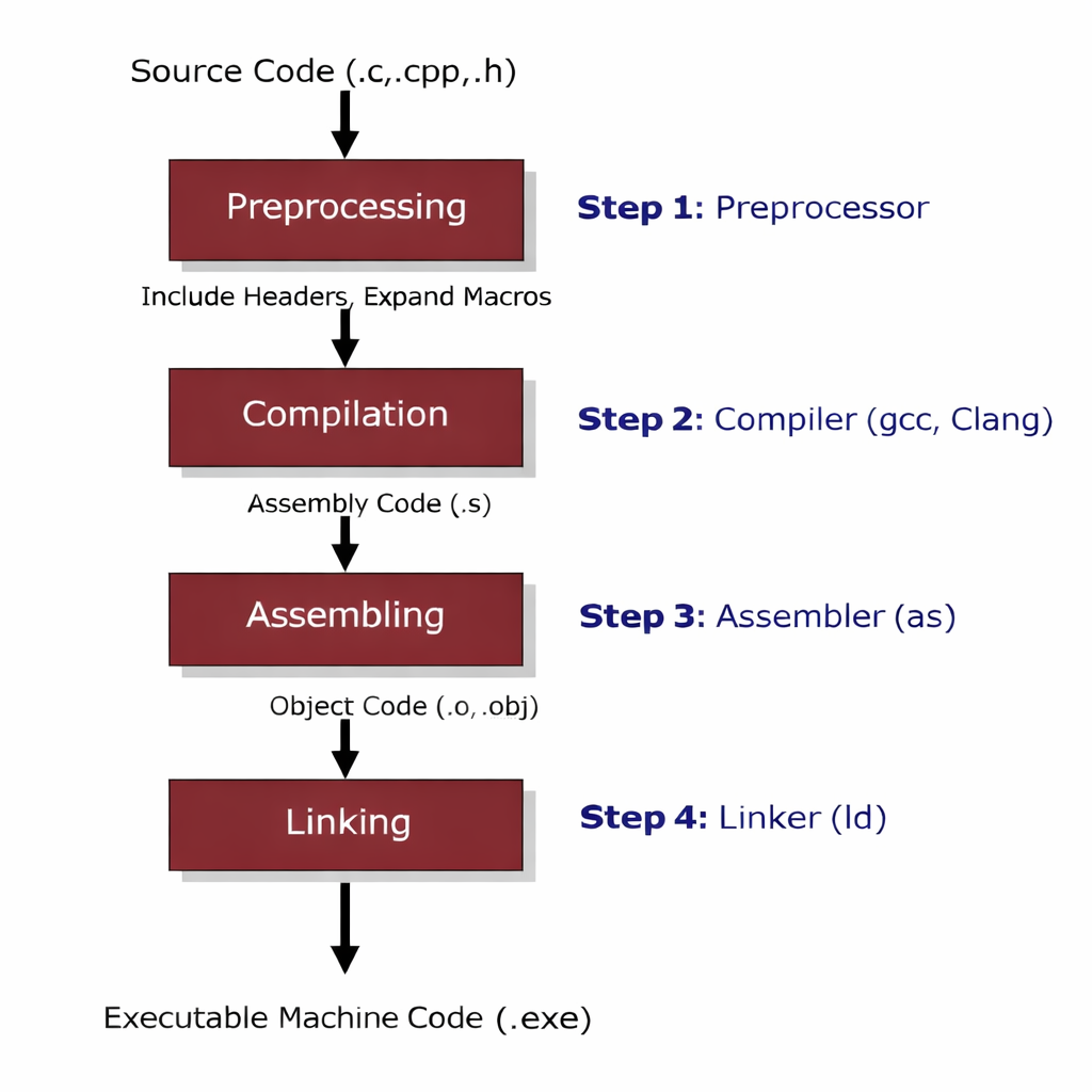
These are the steps involved in producing the final executable, which in this case is firmware that runs directly on the MCU. The linker and startup scripts help with some of these steps, and the Makefile makes the whole process of producing the firmware easier.
Writing a very simple Linker Script#
Unlike a typical desktop or laptop CPU, an embedded microcontroller has a fixed amount of memory. Because of this, the linker must know exactly where each section of the program should be placed within the available memory. This information is provided through a linker script, which is used during the linking stage of the build process.
I wrote a minimal linker script for this project, which can be found here.
NOTE: Typically, the linker script is provided by the MCU vendor or the SDK. I wrote it for learning purposes.
Important things to note about the linker script:
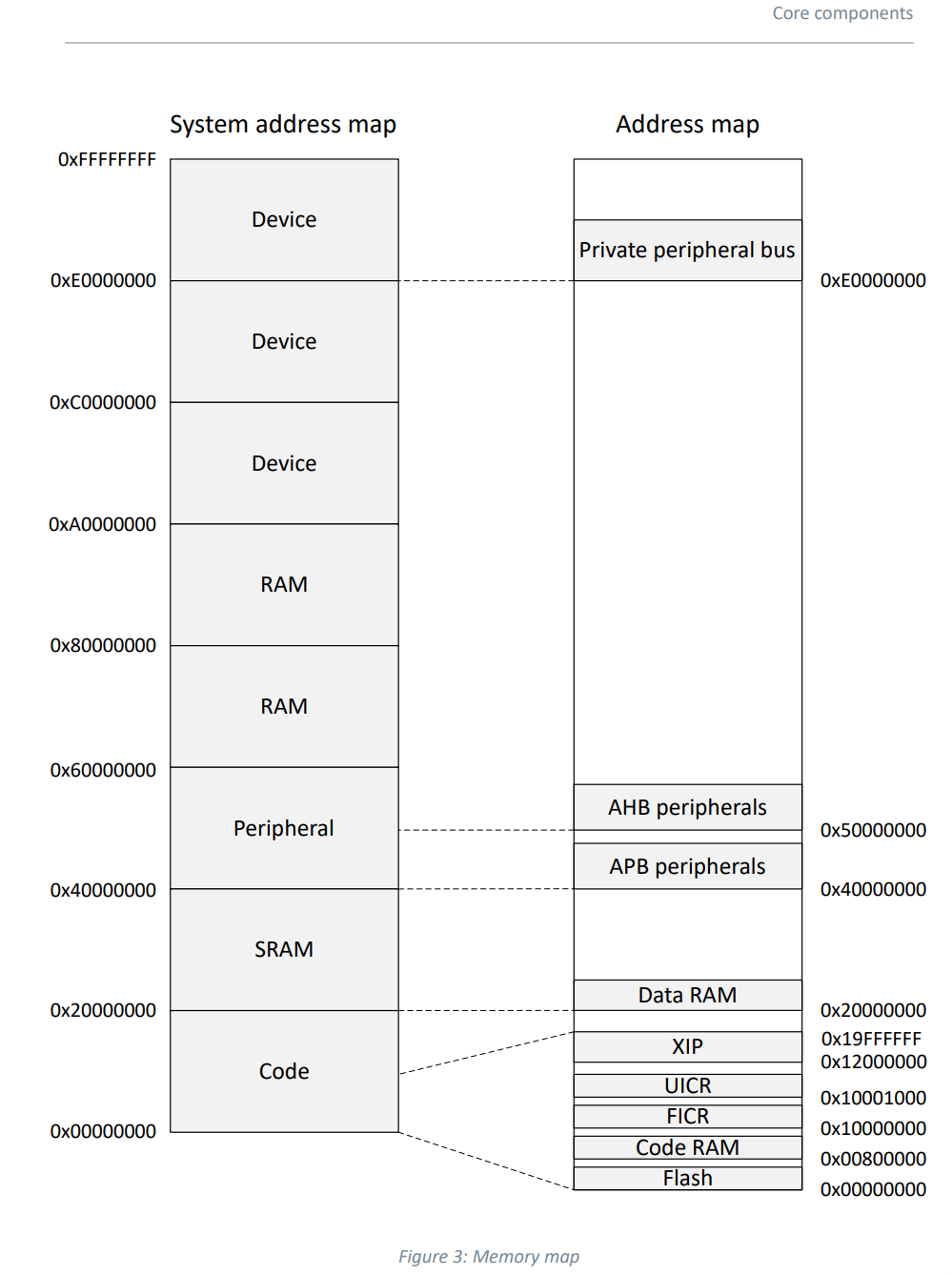
- The MCU has flash and RAM at fixed addresses:
MEMORY
{
  FLASH (rx) : ORIGIN = 0x00000000, LENGTH = 1024K /* r - read, x - execute */
  RAM   (rwx): ORIGIN = 0x20000000, LENGTH = 256K  /* r - read, w - write, x - execute */
}
These addresses can be found in the datasheet
- Placing the stack pointer at the right place in memory to start execution:
/* Initial stack pointer = top of RAM */
_estack = ORIGIN(RAM) + LENGTH(RAM);- The rest of the script is telling the firmware where to keep code and data.
What Runs Before main()#
Unlike a normal program that runs on your computer, the MCU needs to do a startup routine on reset. This can be done using a bootloader (like the Adafruit_nRF52_Bootloader) or in our case we use a small startup script, which can be found here.
NOTE: The startup script is written in assembly language and is typically provided by the MCU vendor or the SDK.
Important things to note about the startup script:
- It contains the Reset_Handler function which
is what executes when the execution starts on the MCU.
Reset Handler copies the
.datasection (which contains initialized global and static variables) from flash to RAM and initializes the.bsssection (which contains uninitialized global and static variables) to zero, then jumps to themain()function. - It also has a Default_Handler function which is a catch-all for any interrupts that are not explicitly defined.
- Apart from these we have a vector table in the script
which points to the appropriate handlers for each interrupt. For example, when the CPU resets, it looks at the vector table to find the address
of the
Reset_Handlerfunction and jumps to it. - For the sake of simplicity, I have not defined any other interrupt handlers in the startup script. In a real-world application, you would typically define handlers for the interrupts you are using.
Building and Flashing the Firmware#
Since we are using a simple Makefile, we can build and flash the firmware using the following commands:
# Build the firmware
make
# Flash the firmware using nrfjprog
nrfjprog --program build/[firmware].elf --chiperase --verify --reset
NOTE: In place of
[firmware]put the name of the binary produced in thebuild/folder.
Details of the Three Experiments#
Blinky: Hello World!#
This is the simplest program that can be written for an embedded system. It configures a GPIO pin and toggles it to blink an LED. Here is the circuit diagram and the demo:
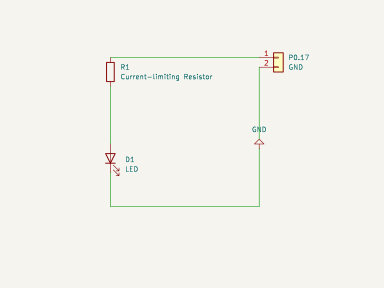
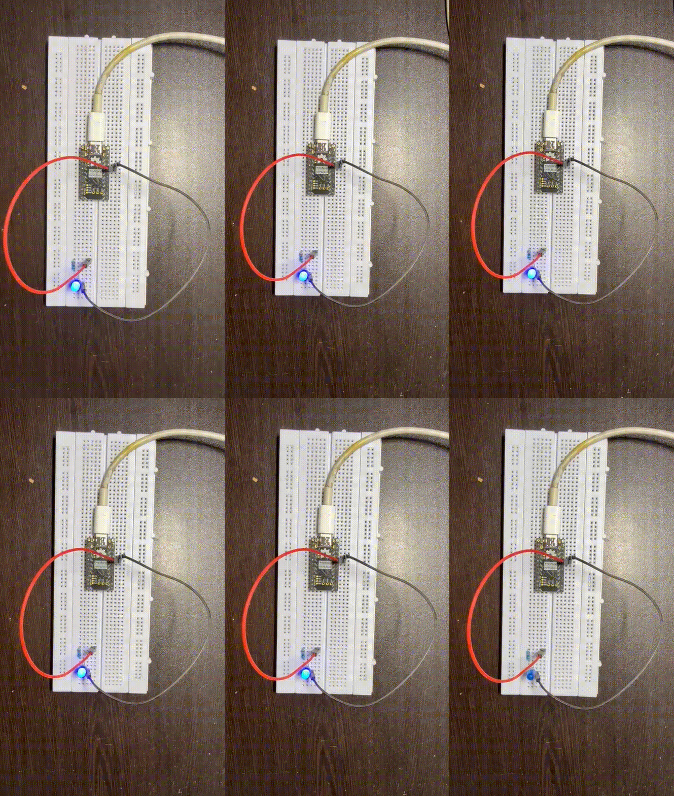
The firmware code can be found here. Important things to note about the code:
- Base address and
OUTandDIRregisters of the GPIO peripheral:
#define NRF_P0_BASE 0x50000000UL

#define REG32(addr) (*(volatile uint32_t*)(addr))

#define P0_OUT REG32(NRF_P0_BASE + 0x504)
#define P0_DIR REG32(NRF_P0_BASE + 0x514)
/*
 * P0 GPIO register addresses:
 *   P0_OUT -> 0x50000000 + 0x504 = 0x50000504
 *   P0_DIR -> 0x50000000 + 0x514 = 0x50000514
 */
The base address and the offsets can be found in the datasheet
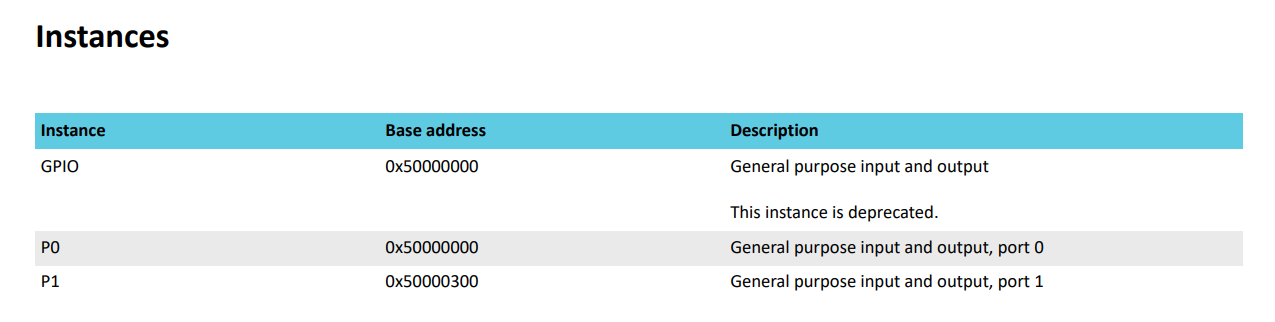
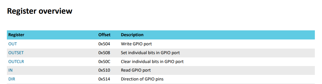
NOTE: For the sake of simplicity, I only use the P0 GPIO peripheral here.
- The GPIO pin needs to be configured as
output before we can toggle it. This is done by writing to the
DIRregister:
#define LED_PIN 17
P0_DIR |= (1u << LED_PIN);
Details
LED_PINis the pin number of the GPIO pin that is connected to the LED. In this case, it is pin 17 (P0.17).1u << LED_PINcreates a bitmask with a 1 in the position of the LED pin and 0s elsewhere.P0_DIR |= (1u << LED_PIN)sets the corresponding bit in theDIRregister to 1, configuring the pin as an output.
- We need a delay function to create a visible blink. Otherwise, the LED will blink too fast for us to see: just a simple
busy-wait loop that executes a number of
nop(no operation) instructions.
static void delay(volatile uint32_t ctr) {
  while (ctr--) {
    __asm__ volatile("nop");
  }
}
The main function: Since it is firmware, it is basically a program that runs forever in an infinite loop and keeps toggling the GPIO pin from high to low with a small delay in between to create a visible blink.
The toggling of the GPIO pin is done by writing to the
OUTregister:
// Set PIN HIGH
P0_OUT |= (1u << LED_PIN);

// Set PIN LOW
P0_OUT &= ~(1u << LED_PIN);
Details
P0_OUT |= (1u << LED_PIN)sets the corresponding bit in theOUTregister to 1, turning the LED on. Similar to theDIRregister.P0_OUT &= ~(1u << LED_PIN)clears the corresponding bit in theOUTregister to 0, turning the LED off.
UARTE (Transmit Only): Minimal Logger#
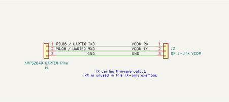
This one taught me a lot of things: what UART is, how to use it to send data to the host, and how to use a logic analyzer to debug the communication. The firmware code can be found here. Here is the circuit diagram and the serial output:
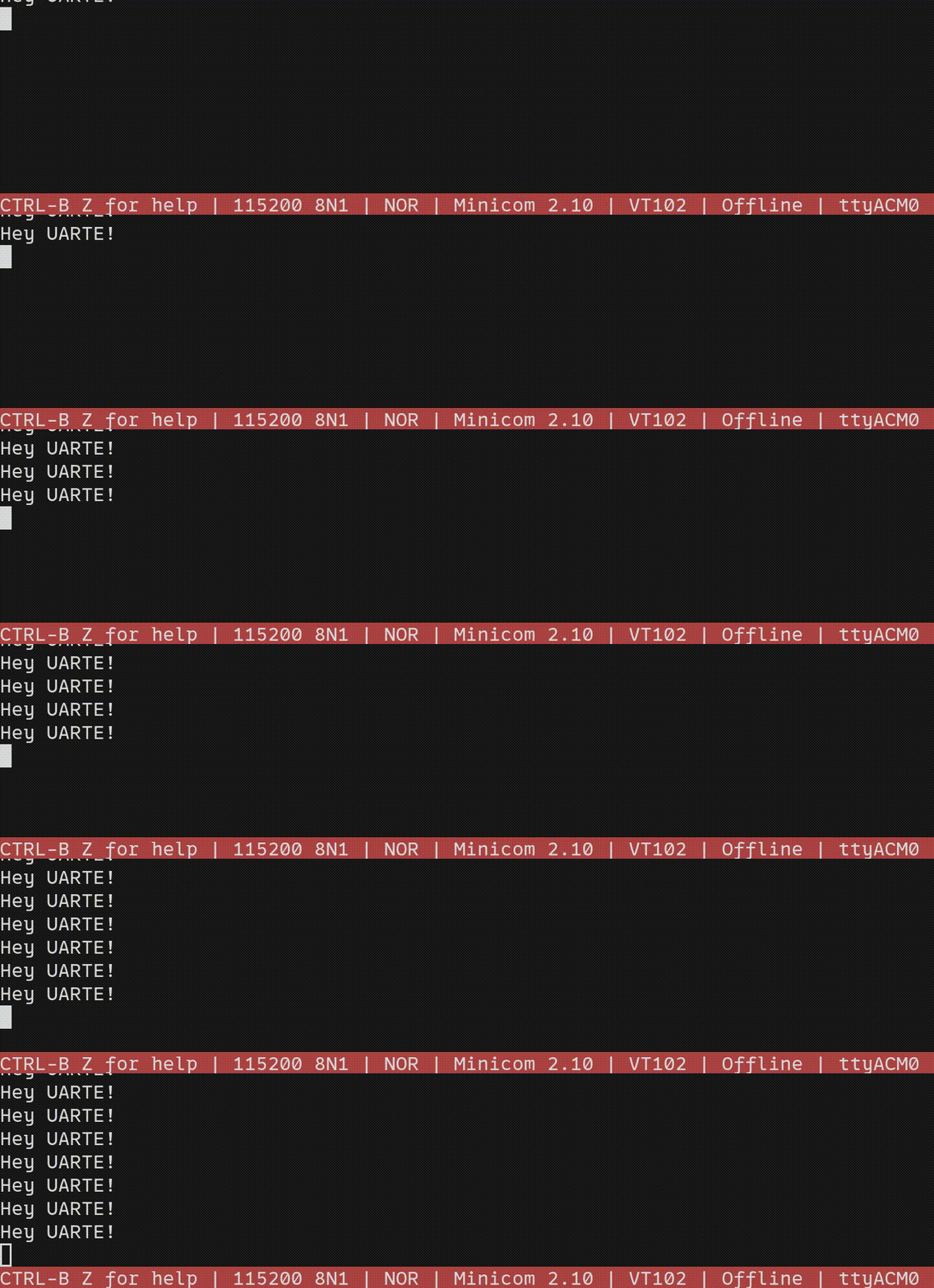
# Command to get the serial output
minicom -D /dev/ttyACM0 -b 115200
NOTE: I did not use an external USB-to-UART adapter for this example. The nRF52840 DK routes the default UARTE0 pins to the onboard J-Link VCOM, which shows up as a serial port on the PC over USB. One of the many benefits of using a dev kit.
UART vs UARTE#
Universal Asynchronous Receiver/Transmitter or UART is a very old protocol for serial communication. UARTE is the Universal Asynchronous Receiver/Transmitter with EasyDMA which is an improvement over the traditional UART. There are plenty of docs on UART and it is quite simple, but here I want to discuss what I learned about UARTE and how I used it to implement this minimal logger in bare-metal. If, like me, you are new to UARTE and EasyDMA, these notes may be helpful:
Notes on UARTE and logger implementation:#
In UARTE, the DMA moves the bytes and the CPU mostly stays out of it. So, we just need to control a few registers for the data to transmit.
Since we are using EasyDMA here, the CPU does not have to manually move every byte. For larger or continuous transfers, hardware flow control can also help avoid overrunning the receiver. This uses two special pins:
- RTS - Request to Send
- CTS - Clear to Send
These are basically specially configured GPIO pins which are enabled by enabling the hardware flow control register (HWFC).
NOTE: For the sake of simplicity I did not use it in the example.
Details
Roughly it works like this:
Device A wants to send data: It asserts RTS -> “Hey, I’d like to send some data.”
Device B checks its buffer:
- If ready, it asserts CTS -> “Go ahead.”
- If busy/full, it de-asserts CTS -> “Wait.”
Device A sends data only when CTS is active.
The data that you want to send needs to be in Data RAM and if it is not in RAM it could cause a HardFault. This is a requirement as EasyDMA can only access Data RAM. To address this we have this:
#define UART_TX_BUF_SIZE 256
static uint8_t tx_buf[UART_TX_BUF_SIZE];
NOTE: This is a writable buffer and writable global/static variables are placed in the
.bsssection (if uninitialized). So, it lives in Data RAM at runtime.
Transmission (TX) process:
- Prepare the transmit buffer in Data RAM and configure UARTE.
- Write the initial address pointer to the
TXD.PTRregister, and the number of bytes in the RAM buffer to theTXD.MAXCNTregister. - Start transmission by triggering the
STARTTXtask. - After each byte has been sent over the
TXDline, aTXDRDYevent will be generated. - Once all bytes of the
TXDbuffer (as specified in theTXD.MAXCNTregister) have been transmitted, the transmission will end automatically and anENDTXevent will be generated. - Stop Manually: Trigger the
STOPTXtask to stop the transmission manually. It generates aTXSTOPPEDevent. - Flow Control: If flow control is enabled through the
HWFCfield while configuring, a transmission will automatically be suspended whenCTSis deactivated and resumed whenCTSis activated again.
NOTE: Since this is transmit-only I will not go into the reception part of UARTE.
Implementation details:
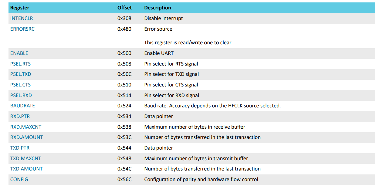
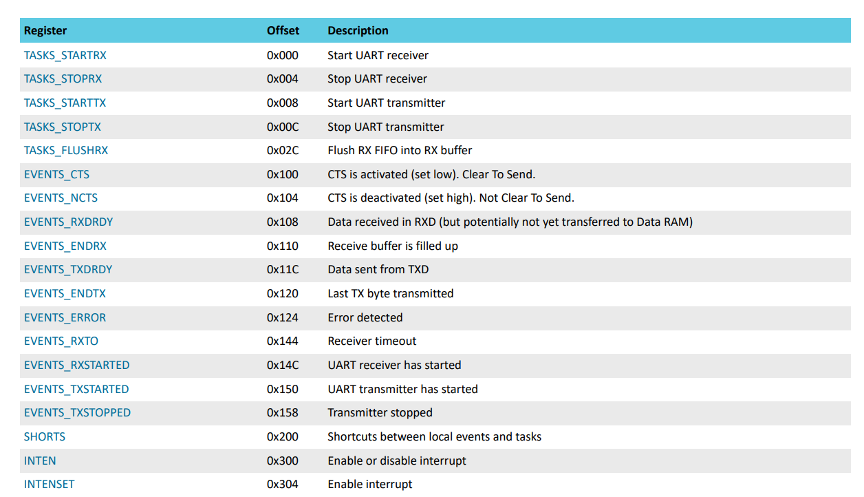
Get access to the registers and tasks as per the datasheet:
#define NRF_UARTE0_BASE 0x40002000UL
#define REG32(addr) (*(volatile uint32_t*)(addr))


#define ENABLE REG32(NRF_UARTE0_BASE + 0x500)
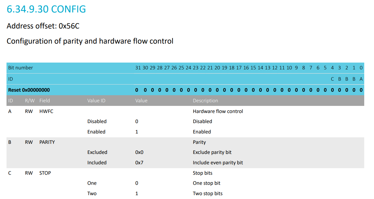
#define CONFIG REG32(NRF_UARTE0_BASE + 0x56C)
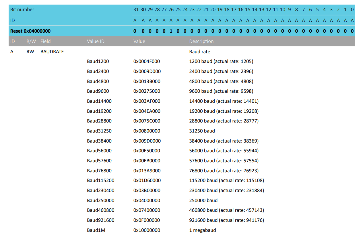
#define BAUDRATE REG32(NRF_UARTE0_BASE + 0x524)
#define PSEL_TXD REG32(NRF_UARTE0_BASE + 0x50C)
#define PSEL_RXD REG32(NRF_UARTE0_BASE + 0x514)

#define TXD_PTR REG32(NRF_UARTE0_BASE + 0x544)
#define TXD_MAXCNT REG32(NRF_UARTE0_BASE + 0x548)

#define TASKS_STARTTX REG32(NRF_UARTE0_BASE + 0x008)

#define EVENTS_ENDTX REG32(NRF_UARTE0_BASE + 0x120)
#define EVENTS_TXSTOPPED REG32(NRF_UARTE0_BASE + 0x158)
Datasheet Reference

Configure GPIO pins and do the pin selection:
#define NRF_P0_BASE 0x50000000UL

// DK: UARTE0 default pins routed to J-Link VCOM
#define TX_PIN 6 // P0.06: UARTE0 TXD -> DK J-Link VCOM RX
#define RX_PIN 8 // P0.08: UARTE0 RXD <- DK J-Link VCOM TX (unused here)

#define P0_CNF(pin) REG32(NRF_P0_BASE + 0x700UL + 4UL * (pin))
Details
The
P0_CNF(pin)macro starts from the GPIO port 0 base address, adds thePIN_CNF[0]offset from the datasheet, and then moves by4 * pinbytes to reach the configuration register for that specific pin. Datasheet Reference:![UARTE datasheet Reference PIN_CNF[0]](../uarte-datasheet-pin-cnf0.png)
P0_CNF(TX_PIN) = (1 << 0) | // DIR = Output
 (1 << 1) | // INPUT disconnect (input buffer not needed for TX)
 (0 << 2) | // PULL = none (field)
 (0 << 8) | // DRIVE = standard (field)
 (0 << 16); // SENSE = disabled

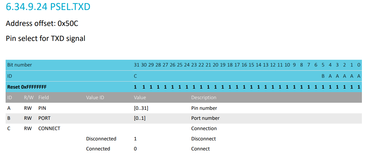
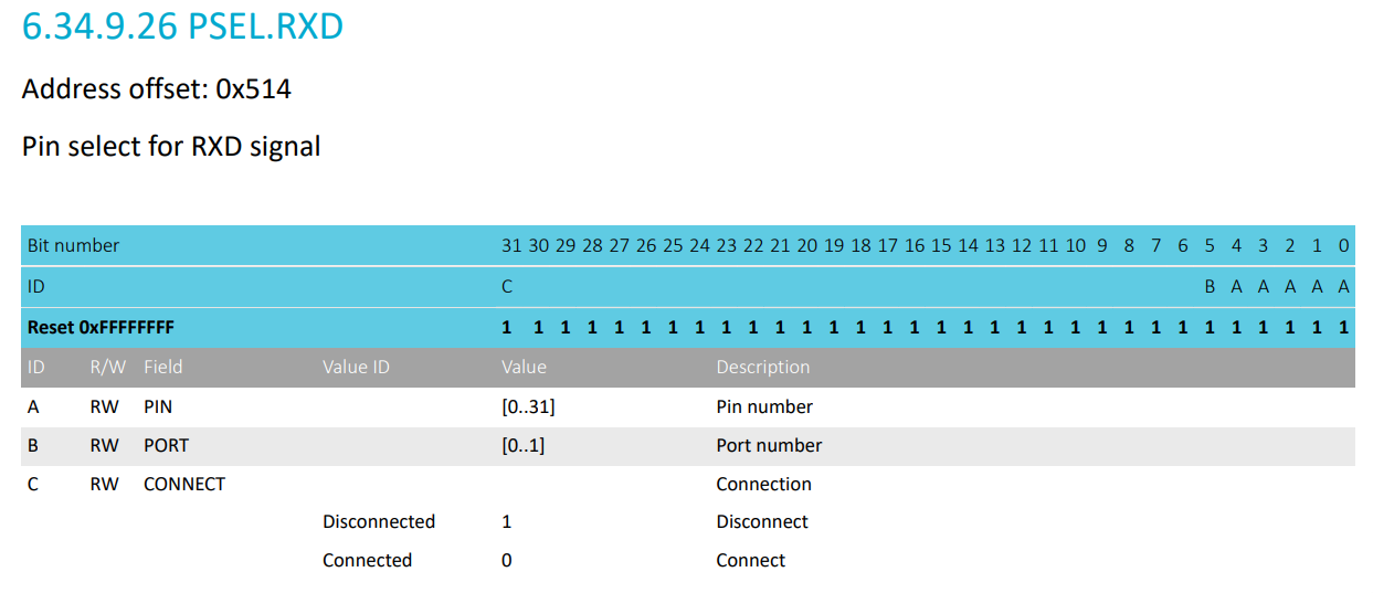
// PSEL format: PIN[4:0] | PORT(bit5) | CONNECT(bit31: 0=connected, 1=disconnected)
PSEL_TXD = (TX_PIN << 0) | (0 << 5) | (0 << 31);

PSEL_RXD = (1 << 31); // RX disconnected (TX-only)
Datasheet Reference
Configure the UARTE peripheral: set baud rate, clear events, etc.
CONFIG = (0 << 0) |   // HWFC disabled
 (0x0 << 1) | // PARITY excluded
 (0 << 4);    // 1 stop bit

BAUDRATE = 0x01D60000; // 115200 (per datasheet table)

EVENTS_ENDTX = 0;
EVENTS_TXSTOPPED = 0;

ENABLE = 8; // Enable UARTE
Datasheet Reference
Sending data over UARTE:
First, copy the string into the RAM buffer by copying the bytes one by one:
for (size_t i = 0; i < len; i++)
    tx_buf[i] = (uint8_t)text[i];
This is needed because UARTE uses EasyDMA, and the transmit buffer should be in RAM. Then, pass that RAM buffer to the UARTE peripheral:
TXD_PTR = (uint32_t)(uintptr_t)tx;
TXD_MAXCNT = len;
Start transmission and wait for it to complete (i.e., wait for the
ENDTXevent):// Start TX TASKS_STARTTX = 1; // Wait for TX to complete - blocking while (EVENTS_ENDTX == 0) { }
Using a Logic Analyzer#
The UARTE implementation also taught me how to use the logic analyzer to debug the firmware. Here is the logic analyzer output of the firmware:

Data sent on TX (as seen in the PulseView output above):
Hey UARTE!\r\n i.e., 0x48, 0x65, 0x79, 0x20, 0x55, 0x41, 0x52, 0x54, 0x45, 0x21, 0x0D, 0x0A
This is the correct data sent over UARTE.
Circuit diagram for connecting the logic analyzer to the DK:
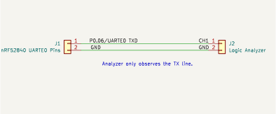
This is quite straightforward. All you need to do is to connect CH1 to the TX pin and connect the GNDs together.
SPI: Sending and Receiving Bytes#
Serial Peripheral Interface, or SPI, is one of the most important protocols for the web server project. The W5500 uses SPI for Ethernet communication, and the SD card uses it for reading and writing data. Before connecting either of them, I wanted to test the nRF52840’s SPIM (SPI Master) peripheral in the simplest possible way: a loopback test. I connected MOSI to MISO, sent a few bytes, and checked whether the same bytes came back. The firmware code can be found here.
Before doing the loopback test, I first checked the data transmission using a logic analyzer. Here is the circuit diagram and the PulseView output for the same:
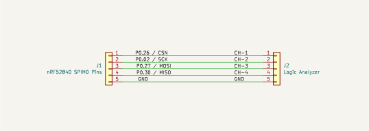
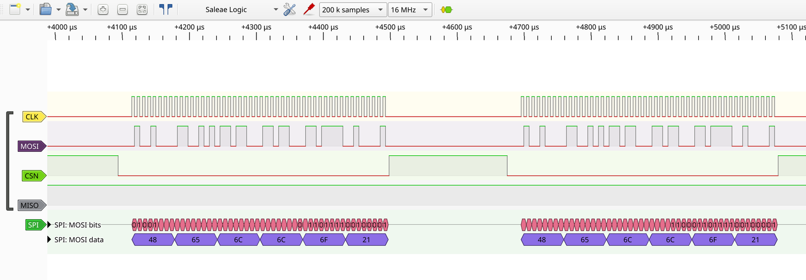
Data sent on MOSI, as seen in the PulseView output above: Hello! i.e., 0x48, 0x65, 0x6C, 0x6C, 0x6F, 0x21. This is the correct data sent
over SPI.
MOSI <-> MISO Loopback Test: Checking the Received Data in GDB#
For the loopback test, I connected MOSI directly to MISO. This means whatever the SPIM peripheral sends on MOSI should come back on MISO. To verify
this from the firmware side, I set a breakpoint after the transfer and inspected the receive buffer in GDB. The buffer contained Hello!, which
matched the bytes sent on MOSI. Here is the output:
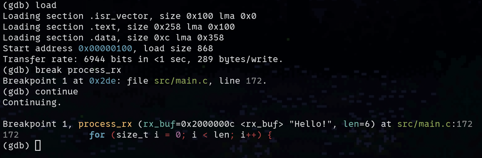
rx_bufSPIM with EasyDMA#
Just like UARTE, SPIM (SPI Master) uses EasyDMA for transfers. There are plenty of articles available on the internet on SPI. So, I will add only a few pointers here.
Important pointers about the implementation:
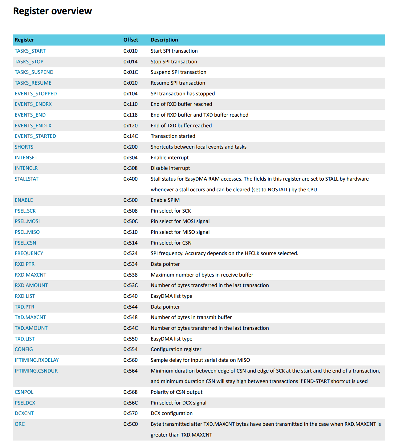
First, we need to get access to the registers and events as per the datasheet:
#define NRF_SPIM0_BASE 0x40003000UL

#define SPIM0_CONFIG REG32(NRF_SPIM0_BASE + 0x554)
#define SPIM0_ENABLE REG32(NRF_SPIM0_BASE + 0x500)
#define SPIM0_FREQUENCY REG32(NRF_SPIM0_BASE + 0x524)
#define SPIM0_TASKS_START REG32(NRF_SPIM0_BASE + 0x010)
#define SPIM0_EVENTS_END REG32(NRF_SPIM0_BASE + 0x118)
#define SPIM0_TXD_PTR REG32(NRF_SPIM0_BASE + 0x544)
#define SPIM0_TXD_MAXCNT REG32(NRF_SPIM0_BASE + 0x548)
#define SPIM0_RXD_PTR REG32(NRF_SPIM0_BASE + 0x534)
#define SPIM0_RXD_MAXCNT REG32(NRF_SPIM0_BASE + 0x538)
Datasheet Reference

Since SPI is full-duplex: for every byte you transmit on MOSI (Master Out, Slave In), the peripheral also receives one byte on MISO (Master In, Slave Out). And since this is a loopback, each transmitted byte should come back into the receive buffer. So, we keep both sizes the same:
// Hardcoded for demo purpose!
static uint8_t tx_buf[] = {0x48, 0x65, 0x6c, 0x6c, 0x6f, 0x21}; // "Hello!"
static uint8_t rx_buf[sizeof(tx_buf)];
Configure the SPIM peripheral by configuring GPIO pins for all the lines, setting SPI mode, endianness, and SPIM frequency. This is very similar to the UARTE one. Just look up the values needed in the datasheet and use those.
NOTE: To keep things simple I chose SPI mode 0 with MSB first for this project.
To send and receive data, all we need to do is point to the transmit buffer (
tx_buf) and the receive buffer (rx_buf) in Data RAM just like in UARTE. And we need to point the registers to the correct places accordingly:SPIM0_TXD_PTR = (uintptr_t)tx_buf; SPIM0_TXD_MAXCNT = sizeof(tx_buf); SPIM0_RXD_PTR = (uintptr_t)rx_buf; SPIM0_RXD_MAXCNT = sizeof(rx_buf);Apart from this everything is very much like the UARTE implementation.
One different thing I tried here was making the SPI transfer non-blocking at the application level. Instead of starting the transfer and immediately waiting in a
whileloop until it finished, I start the transfer once, mark SPI as busy, and then keep checking theSPIM0_EVENTS_ENDevent inside the main loop.if (spi_busy == 0) { start_spi(); spi_busy = 1; }When the transfer completes, the SPIM peripheral sets
SPIM0_EVENTS_END. At that point, I clear the event, deassert chip select, mark SPI as free again, and send the receive buffer for inspection.if (SPIM0_EVENTS_END) { SPIM0_EVENTS_END = 0; csn_high(); spi_busy = 0; process_rx(rx_buf, sizeof(rx_buf)); delay(1000); }This is a polling-based implementation.
NOTE: For this experiment, I kept it polling-based because the goal was only to understand how the SPIM task/event flow works. A real driver would usually avoid checking the event register forever and would handle transfer completion using an interrupt instead.
Try It Yourself#
If you are also starting with embedded systems, I would suggest trying small experiments like these yourself. The GitHub repo READMEs have the details needed to run the examples.